


PCB And Circuit Design Certification Training
Discover the depths of PCB And Circuit Design Technology. Join us now to gain comprehensive insights into PLC & Scada technology from a seasoned professional.
![]() 5 out of 5 based on 101 user reviews. |
5 out of 5 based on 101 user reviews. |  |
|  |
|  |
| 
Enquire Now
Accreditations & Affiliations

Training Features

Instructor-Led Sessions

Real-Life Case Studies

Assignment

Live Projects

Connect with 2 Lakh + Alumni

Govt. Recognized Certification

Dedicated Placement Support

App-Based Learning

A CMMI Level 5 Company
Best PCB and Circut Design Training Institute in Delhi NCR
Join Best Pcb & Circuit Online Training in Delhi, Pcb & Circuit Online Training Course in Delhi, Pcb & Circuit Online Training Institute in Noida
PCB (Printed Circuit Board) is a thin board of fibreglass or laminated material in which self- contained interconnected electronic components are found. It electrically connects and mechanically supports all the electrical components. It is done by using conductive tracks or through the laminated copper sheets.
It is found in beepers, pagers, radars or computer systems. The applications of PCB can be found in desktop and laptop computers, video cards, controller cards, network interface cards and expansion cards. PCBs can be divided into three categories on the basis of copper layers:
- Single Sided (only one layer).
- Double Sided (two layers).
- Multi-layer (more than two layers).
PCBs are usually green in colour. In case of advanced PCB the components such as capacitors, resistors or active devices can be present.
- 1947 : The development of early PCB can be traced back to 1920, but it was in 1947 when double sided PCB came into being which contained plated through holes.
- 1957 : Formation of IPC (Institute of Printed circuits) took place.
- 1960 : Production of Multilayer (4+ layers) PCB began.
- 1960-1970 : Boards were designed using 4:1 red and blue line vellum method, and the circuitry and overall size of the boards were becoming smaller, and hot air soldering methods began to be used.
- 1992 : Genesis 2000 software for PCB, CAM and DFM was founded by Valor Computerized systems.
- 1995 : Implementation and use of micro-via technology in PCB production started, hence HDI (high density interconnects) PCB came into existence.
- 1997 : ODB++ printed circuit board manufacturing data was released by valor computerized systems.
- 2010 : The production of ELIC (Every layer Interconnect) begins.
For Interconnecting and packaging of the electronics components of the product, PCB forms the “basic foundation”. This fact clearly states that it’s an evergreen branch as the need for designing the equipment in different sectors will always be there.
The demand for PCB in the automotive sector has risen rapidly, as the automobile industry has large number of electrical component embedded in their structure. There has been rapid growth in Electronics and manufacturing industry, due to boom in the field of telecom industry, gaming industry and consumer electronics which in turn has led to the remarkable development in the last two decades.
Engineering Students can start their career in this field by joining PCB Training from a reputed institute. PCB designers find crucial role in R&D (research and Development) units, in electronic production units as well as in PCB industry. Since this sector is highly technical, the pay package is very good right from the fresher level.
- The basic concepts of physics or basic electronics such as voltage, current, power etc. must be crystal clear.
- Knowledge about the materials such as copper, gold and aluminium can help the students in implementing the concepts.
- The basic component of electronics is divided into active and passive components which are studied thoroughly.
- After that Circuit designing using the given components is done and practical knowledge is gained.
- Then the simulation (circuit is run on software) is done to achieve the desired expertise.
- Finally, PCB layout designing using PCB express or eagle is done and executed.
CETPA, the leader in “high end technologies” has a rich experience of 12 years in providing PCB Training to students. CETPA is a training school for higher learning and training in embedded system design, PCB Design and VLSI technologies with its training centres in Noida (Delhi-NCR), Roorkee, , Dehradun and Lucknow. It offers vocational PCB training courses for working professionals and six months PCB training course for students.
The domains covered are:- PCB Printing and Etching
- Drilling and Soldering
- Express SCH and Express PCB
- Proteus
CETPA trains students in two types of software such as Student Level software (Express PCB) and Professional level software (Eagle). Rigorous knowledge is given to students on each of the domains so that innovative components can be built meeting the industry and visionary world. Special emphasis to some CAD software for PCB such as Pad2Pad, multisim, Eagle is given to develop a good knowledge base of the students. The labs are excellent and provide superb environment for practical learning and developing skills in lucid and simple manner. Some worth mentioning features are:
- The company has superb structured course content designed which includes CAD software’s for PCB Training.
- The company has expert trainers who assist the students in innovative projects.
- Students get practical exposure by getting access to technologically updated CETPA labs.
- CETPA’s syllabus for PCB Training is professionally designed to cover basic as well as advance aspects of PCB & Circuit Designing.
- Technical training is well planned to provide students with Theoretical as well as Practical Knowledge of the module.
- Online classes for benefit of NRI students and also for those who have no CETPA training centre in their region.
PCB market has managed to expand globally, thanks to the rapid expansion of the electronics manufacturing bases. It is impossible to imagine the design of a circuit without PCB concepts. Hence, PCB sector is loaded with loads of career opportunity for the professionals. Below given are some of the eminent companies implementing the concepts of PCB:
- Cirexx International
- Advanced Assembly
- Dell
- Intel
- IBM
Students should focus on developing the innovative skills in circuit designing because this field rests on “out of the box thinking”. Hence, students should join CETPA for PCB Training course to develop out of the box thinking and fulfil their career demands.
CEATPA offer industrial training and internship program to help students and professionals by providing them end-to-end recruitment of right professionals as per requirement of the industry. CETPA has a well established placement consultancy firm which has proven track record of superb placements in top-notch companies like:
- Sony India
- Multivirt technologies
- EA Sports (to name a few...).
CETPA trains student to be Industry ready in India as well as foreign based companies and this is reflected in our placements. Students willing to bag a good and exciting career can join CETPA for an exciting experience. For a countless number of placements from CETPA please Click Here.CETPA trains student to be Industry ready in India as well as foreign based companies and this is reflected in our placements. Students willing to bag a good and exciting career can join CETPA for an exciting experience. For a countless number of placements from CETPA please Click Here.
- You will get better knowledge of programming and how to implement it for actual development requirements in the industrial projects and applications.
- Enhanced knowledge on the web development framework. Using this framework, you can develop dynamic websites swiftly.
- You will learn how to design, develop, test, support and deploy desktop, custom web, and mobile applications.
- Design and improve testing and maintenance activities and procedures.
- Design, implement and develop important applications in a Pcb And Circuit environment.
- Increased chances of working in leading software companies like Infosys, Wipro, Amazon, TCS, IBM and many more.
Professional growth, increased compensation and validation of the skill are the most popular reasons why individuals and professionals seek IT certifications. Keeping this in mind, we at CETPA provide you with certification in latest and innovative technologies to help you to reach your certification goals.
CETPA is the official Training partner of Oracle, Microsoft, Autodesk, Panasonic and Nuvoton and thus provides Training as per international standards and curriculum. CETPA proudly provides you certification in association with our training partners so that you can validate your domain specific technical skills. Certification from these big brands will help you in grabbing your dream job.
- Gives you an advantage while searching for a job and provide a competitive advantage over your competitors.
- Ensure knowledge and skill are up to date and can be applied to the job
- Provide credibility to those looking for a career in an IT domain.
- Offer fast track to career advancement
- Demonstrate level of competency
- Professional Credibility as well as it demonstrates your dedication and motivation to professional development.
- You are likely to stand out from the crowd and be considered to be successful in your positions.
- Represent a well-recognized and valued IT credential that increases marketability and competitive edge.
- Provide peace of mind with the confidence that certified employees have truly learned the skills necessary to do their jobs;
- Express valuable credentials to search for in prospective employees, and can help retain top performers when offered as an incentive;
- Offer a competitive advantage when the team is trained and certified regularly.
Talk To Advisor
MODE/SCHEDULE OF TRAINING:
| Delivery Mode | Location | Course Duration | Schedule (New Batch Starting) |
|---|---|---|---|
| Classroom Training (Regular/ Weekend Batch) | *Noida/ *Roorkee/ *Dehradun | 4/6/12/24 Weeks | New Batch Wednesday/ Saturday |
| *Instructor-Led Online Training | Online | 40/60 Hours | Every Saturday or as per the need |
| *Virtual Online Training | Online | 40/60 Hours | 24x7 Anytime |
| College Campus Training | India or Abroad | 40/60 Hours | As per Client’s need |
| Corporate Training (Fly-a-Trainer) | Training in India or Abroad | As per need | Customized Course Schedule |
Course Content
INTRODUCTION TO CIRCUIT DESIGNING
- Need of Circuit Designing
- Introduction to Electronic Components
- How to Select Components
- Basic Circuit Designing Process
- Types of PCB’s used
- The Designing Process
INTRODUCTION TO CIRCUIT SIMULATION TOOL
- Exploring the Simulation Tool
- Adding and Exploring Component Libraries
- Creating 5VDC Multivibrator Circuits
- Adjusting Voltage, Current and Values of Components
- Creating 220VAC Power Circuits
- Connection Troubleshooting
- Exploring the Designing Tool
- Loading components in Library
- Working on component schematic
- Working on component footprint
- Working on component 3D model
- Working on Annotations Marking
- Schematic sheet Setup
- Placing components in schematic
- Annotation of the components
- Routing the schematic
- Working on net class
- Adjusting Net Parameters
- Working on port connections
- Multiple sheet schematic
- Design rule check
- Adding text
- Shape and image
- Troubleshooting Warnings and Errors
- Generating Netlist
- Printing Schematics
- Configuring the Circuit Board
- Understanding the Board Layers
- Placing components in layout
- Routing the components
- Working on Copper Pouring
- IPC Standard Rules and Conventions
- Multiple Layer Routing
- Placing Ground and Power Planes
- Design rule check
- Adding text, shape and image
- Troubleshooting Warnings and Errors
- Generating Gerber Files
- Generating N/C Drill Files
- Working on 3D View
- Generating 3D View Files
- Printing the Layout
- Developing copper clad layout
- Etching the clad
- Drilling for holes
- Mounting components and soldering
- Troubleshooting

Our Process


FAQ'S
- Classroom Training
- Online Training
- Corporate Training
- On campus Training
Career Assistance
- Build an Impressive Resume
- Attend Mock-Up Interviews with Experts
- Get Interviews & Get Hired
Training Certification
Earn your certificate
Your certificate and skills are vital to the extent of jump-starting your career and giving you a chance to compete in a global space.
Share your achievement
Talk about it on Linkedin, Twitter, Facebook, boost your resume or frame it- tell your friend and colleagues about it.

Upcoming Batches
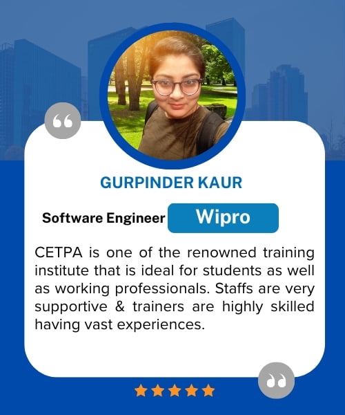
What People Say
Our Partners


Need Customized Curriculum? Request Now
Structure your learning and get a certificate to prove it.

Our Clients


Our Placed Students


Review Us
Anunay Mailk
![]() Friday, 14 April 2017
Friday, 14 April 2017
PCB Training In Noida
The best place to learn any technology. If you want to excel in PCB join CETPA. You can learn and implement your learning by working on live projects.
Course Features
- Lectures 0
- Quizzes 0
- Duration 10 weeks
- Skill level All levels
- Language English
- Students 0
- Assessments Yes


